Making Custom PCBs
We've all see something like this before.
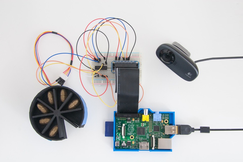
The simple breadboard with a messy, beautiful rainbow of wires sticking this way and that. This part of a project is where I control a stepper motor, which tells the dispenser to twist the fan looking thing and dispense a treat. Luckily, Adafruit has published this exact tutorial. So I followed the Adafruit tutorial and plugged in a whole bunch of wires where the tutorial told me to plug. Easy enough! But now, how does one tidy things up?
Why, printed circuit boards, of course! You know, those green things with lines all over them. Don't worry. It's not that hard.
Meet Fritzing, your friendly PCB designer
Fritzing is kind of like LEGOs of PCB design. It's simple, good for learning. A stepping stone to Eagle or KiCAD.
Step 1: Virtual Breadboard
This is my favorite part of Fritzing. As a novice hardware hacker, it helps that I start with something I already have working: breadboards and jumper wires.
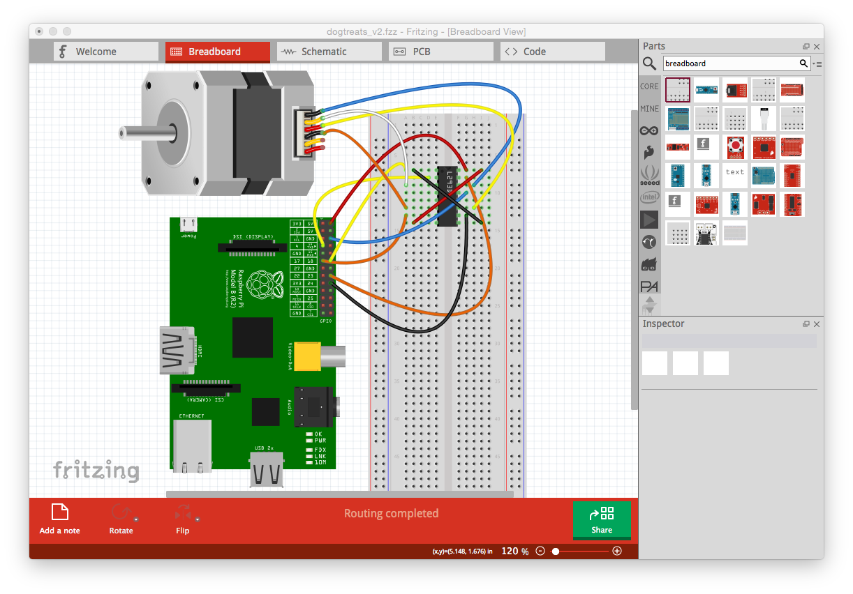
With Fritzing, you start with a virtual breadboard set up. Click the "Breadboard" tab. Here, you can search for various components, like "breadboard" and "Raspberry Pi" and "L293D" (the motor driver I used).
Add components to the workspace. Then click to start dragging wires around. Protip: press the control (Windows) or cmd (Mac) key to make the wires all bendy... just like in real life.
Step 2: Schematics
If you switch to the Schematics tab, you'll see an outline of the schematics. But... I didn't really deal with this view very much. So let's skip it. =P
Step 3: PCB
Now we get to the fun part! When you open up the PCB view, you should see something like this.
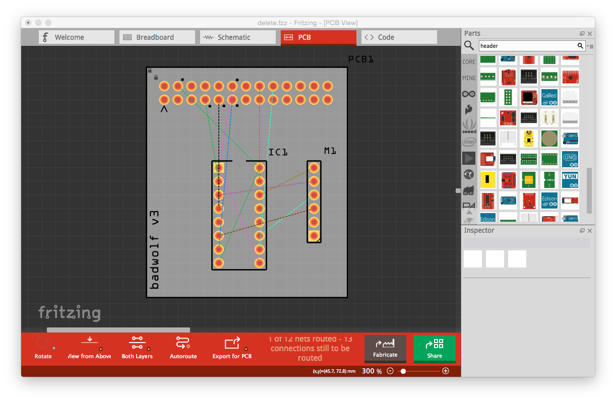
This is just the components you selected. Well, they are holes to plug in the components you selected.
The dotted lines represent where the connections should go. Our goal is to turn these dotted line (airwires) into routes. To do this, just drag a dotted line into place.
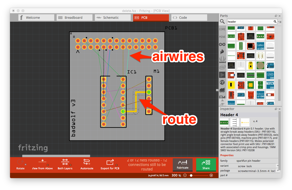
The goal is to create a board without any routes criss crossing with another route. That would be bad. Electricity would ram into one another and we will not have a good time.
One way to tackle this is to use multiple layers. For me, 2 layers was sufficient to route all the airwires without anything crossing.
To connect a route on the top layer with one on the bottom layer, you use via. As in, go from top to bottom via this connection. To do this add a bend point by right clicking on route then clicking "Add a Bendpoint." Then, right click on the bend point and choose "Convert Bendpoint to Via." Then you can right click on different parts of the route to move between layers.
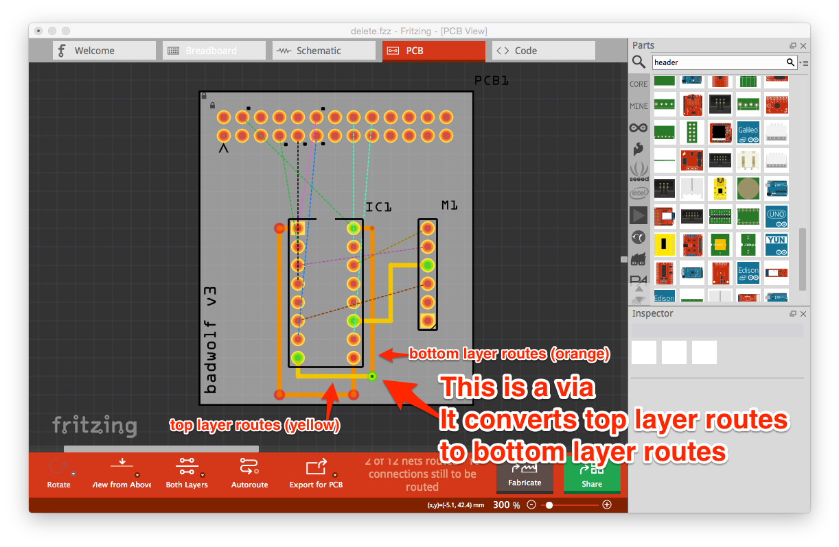
Eventually, all your routes come together nice and cleanly. You can check that your routes are indeed error free by using the nifty design checker (Tool Bar > Route > Design Rule Check).
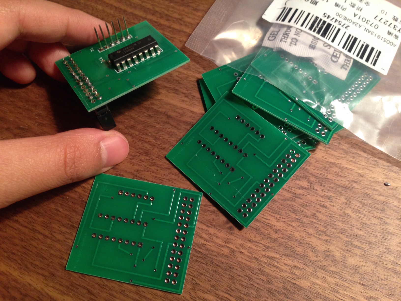
I ended up with something like this.
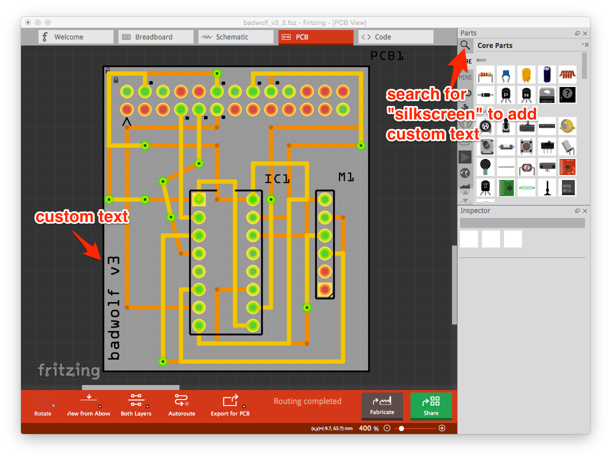
The dots on top is just a marking I made to tell me which pins I need to solder. Or more importantly, which pins I can use as practice. My soldering skills are... lacking.
You can add text (like the dots or the "badwolf v3" in the bottom left) by searching for "silkscreen" under the Parts section in the right toolbar.
Production
Now that we have a PCB sketch, let's get to making.
What I ended up doing is exporting to Gerber files. It's a series of files that tells the machine where to drill holes, how to label things, and of course where to put down the copper so your precious electricity can flow to their rightful homes.
You can preview your Gerber files to make sure they work using GerbLook.
PCB Prototyping Companies
I did a few searches, and found some good options. This is based on:
- shipping to Seattle
- 2 layer board
- board that measures 1.5x1.75 in2.
Actual mileage may vary depending on your design.
| Company | QTY | Lead Time (to Seattle) | Price | Limits/Pricing |
| OSHPark | 3 | 10-14 business days 8-12 production + 2 shipping | $12 $12 PCB + $0 shipping | $5/in2 |
| PCBNet | 1 | 9 BDs 5 prod + 4 shipping | $25 $25 PCB + $0 shipping | under 60in2 |
| ITEAD | 10 | 6 BDs 4 prod + 2 shipping | $28 $10 PCB + $18 shipping | under 5x5cm2 |
| ITEAD | 10 | 20 BDs (could be longer) 4 prod + 16-? shipping | $15 $10 PCB + $5 shipping | under 5x5cm2 |
| SeeedStudio | 1 | 18-48 BDs 3 prod + 15-45 shipping | $15 $10 PCB + $5 shipping | under 5x5cm2 |
| SeeedStudio | 1 | 5 BDs 3 production + 2 shipping | $40 $10 PCB + $30 shipping | under 5x5cm2 |
| Fritzing | 1 | 17-25 BDs 7-11 production + 10-14 shipping | $21 $17 PCB + $4 shipping | $5.20 + $0.96/cm2 |
In the US, the fastest/cheapest seem to be OSHPark if you have small boards. OSHPark (stands for open source hardware park) charges by the square inch. So if you have a tinyass board like my dog treat thing, it's only $12 or less. If you have a 3x3in2 board though, it's $45, even though each side only doubled in length. Yay. Behold the power of exponents.
I ordered from ITEAD. Paid a little extra for DHL Express. Still, it came down to about $3/PCB since they ship 10 QTY. I did end up having to use an extra PCB because I'm apparently the kind of idiot who solders things backwards the first time around.

Not bad, eh?
Ok. Now go and make stuff.